Joint Development Programs
Functional Nanofilms
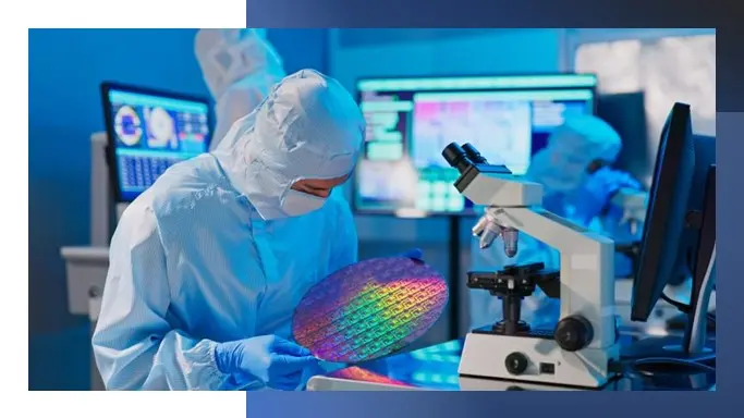
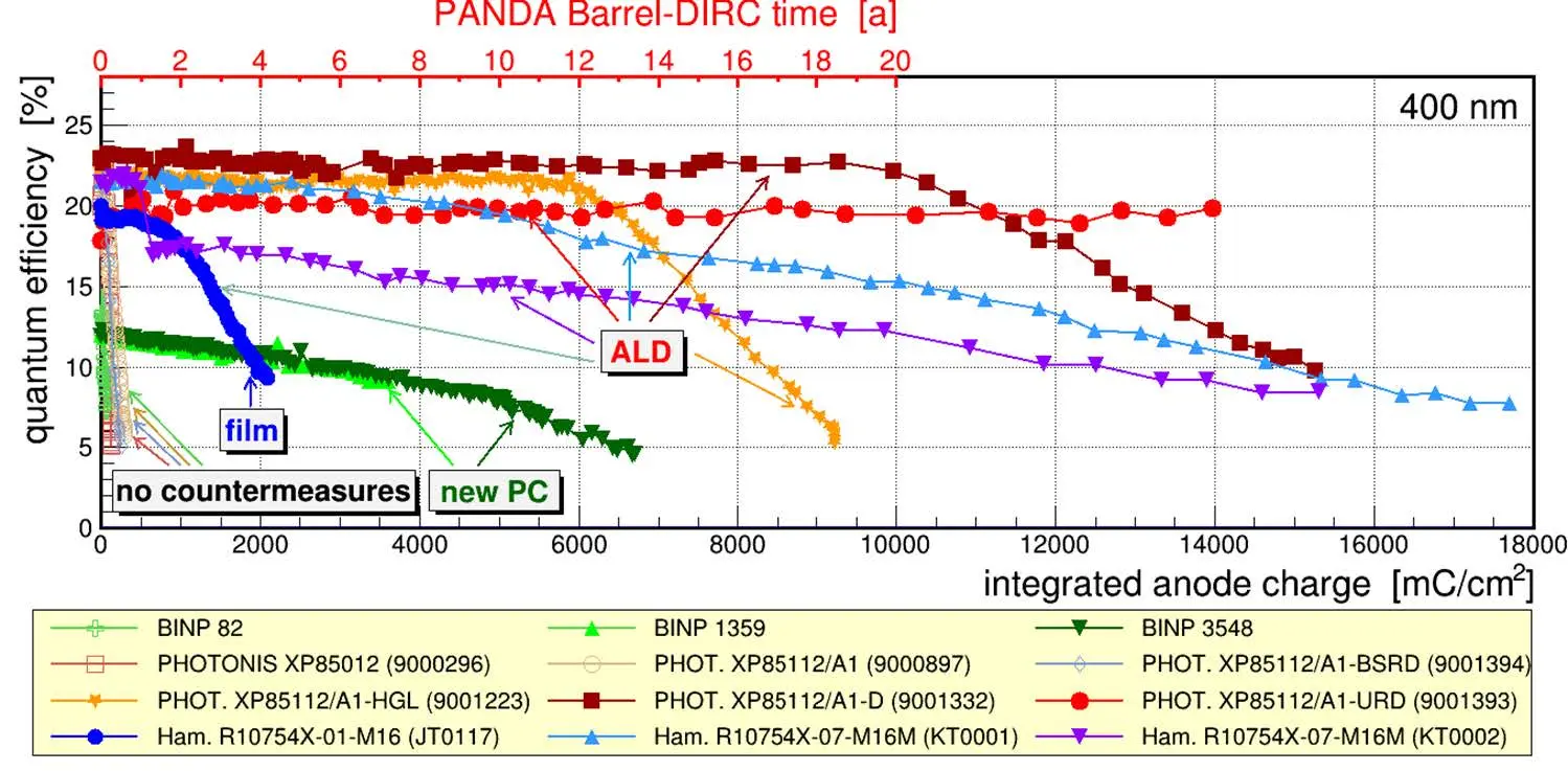
Conductive and Secondary Electron Emissive nanofilms for Microchannel Plates (MCP)
Development of Functional Nanofilms, enabling revolutionary substrate independent Microchannel plate (MCP) devices, possessing long lifetimes and superior temporal and spatial resolution that will transform High Energy Physics. Arradiance has successfully licensed this technology, protected by 12 issued US patents (with several US and international Patents pending) to leading detector manufacturers (Hamamatsu, Incom and Photek). The technology is being implemented in HEP programs world-wide, such as BELLE in Japan and DIRC in Germany
Arradiance United States Patents: 9368332, 9064676, 8237129, 8227965, 8134108, 8052884, 7977617, 7855493, 7759138, 7408142, 6522061, 5729244
Joint Development Programs
Nanofilm for solid oxide fuel cell (SOFC)
Yittria stabilized zirconia (YSZ)
The film requirements included HAR (500:1) and HSA (7m2 per wafer) for the platinum particle reactor bed. SOFCs are defined by the use of a solid ceramic oxide as the electrolyte membrane: typically Yttrium-Stabilized Zirconia (YSZ). Maximizing the power density that the SOFC can produce requires operation at high temperatures. To accomplish this, electrode performance is improved by increasing the density of active electrode sites, using more catalytically active materials and minimizing the electrolyte resistance by reducing film thickness. This optimization is well suited to the capabilities of ALD. Target YSZ thickness 15nm, target material ratio 94:6
(ZrO2:Y2O3). Rutherford Backscatter results show low C and N contamination (1%) and material ratio of 93.7:6.3. XPS analysis of YSZ film shows good stoichiometry and excellent conformality over the entire aspect is shown in the composite micrograph above right.
Joint Development Programs
Conducting and insulating Nanofilms
Super capacitor
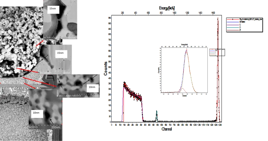
The device (US Patent 9,012,092) is comprised of a compressed wire mesh material that creates a HAR (greater than 1000:1) and HSA (greater than 1.5m2) device that is characterized by a high specific capacitance that results from a layer of a dielectric material sandwiched between two conductors all of which are formed by ALD on wire mesh "scaffolding". ALD ensures that the conducting and dielectric layers of the capacitor possess surface areas comparable to the wire mesh scaffold, resulting in a relatively large value for the surface area which is proportional to the device capacitance. The conformal and uniform ALD dielectric allows for small film thickness, which is inversely proportional to the capacitance. This combination, enabled by ALD, result in a large specific capacitance and a large specific operating charge. Using Arradiance proprietary surrogate substrate techniques, ALD Al2O3 and Pt nanofilms films were developed that defined the capacitive structure within the compressed wire mesh device. A mechanical cleave allowed imaging of the ALD coated wire structure deep within the device as shown in the SEM images above.
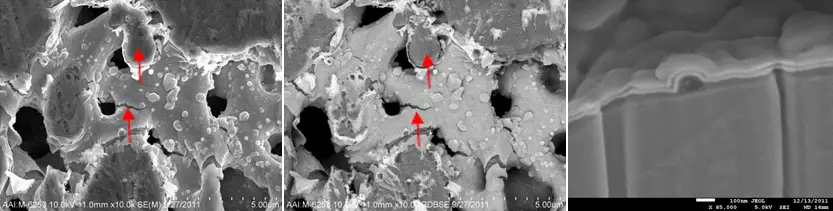
The leftmost image is a secondary electron image showing exposed wire (upper arrow) and a crack in the ALD layers due to the cleave. The right image is a backscatter electron image that shows the material (atomic number) contrast between the wire material (upper arrow) and the Pt ALD film (lower arrow). These images show the successful coating of the functional ALD layers deep within the HAR / HSA device structure. A FIB cross-section of an individual wire is shown in the figure above right, where it is possible to see the multilayer films that make up the super capacitor's microstructure.
Joint Development Programs
XRAY optical coatings
Space and Terrestrial applications
XRAY mirrors, Optical components and Lobster Eye implementations. Compton (1923) demonstrated X-rays could be reflected off of a polished surface if the angle of incidence of the incoming photon was kept very small (~1o). In addition to the requirement for grazing incidence, realization of the enormous gain in resolution that X-ray microscopy affords, due to its short wavelength, is difficult because the process of focusing x-rays requires that the surface of the mirror be extremely smooth: up to 20% of the x-ray photons scatter if the surface roughness is of the same dimension as the x-ray photon wavelength, on the order of 1 Angstrom. X-ray imaging requires extremely smooth, aspheric grazing incidence mirrors in which a beam of X-rays is reflected and the intensity is measured in the specular direction. Focusing of X-rays requires that a reflection from a parabolic mirror is followed by a reflection off a hyperbolic mirror. This limits the collecting area since the incoming X-rays must strike the tilted surface of the mirror.
A small improvement to collection area can be achieved by a nesting arrangements of mirrors inside each other. Newer designs, such as the Lobster eye (Below) can significantly increase collection area in a reduced form factor at a small expense to resolution.
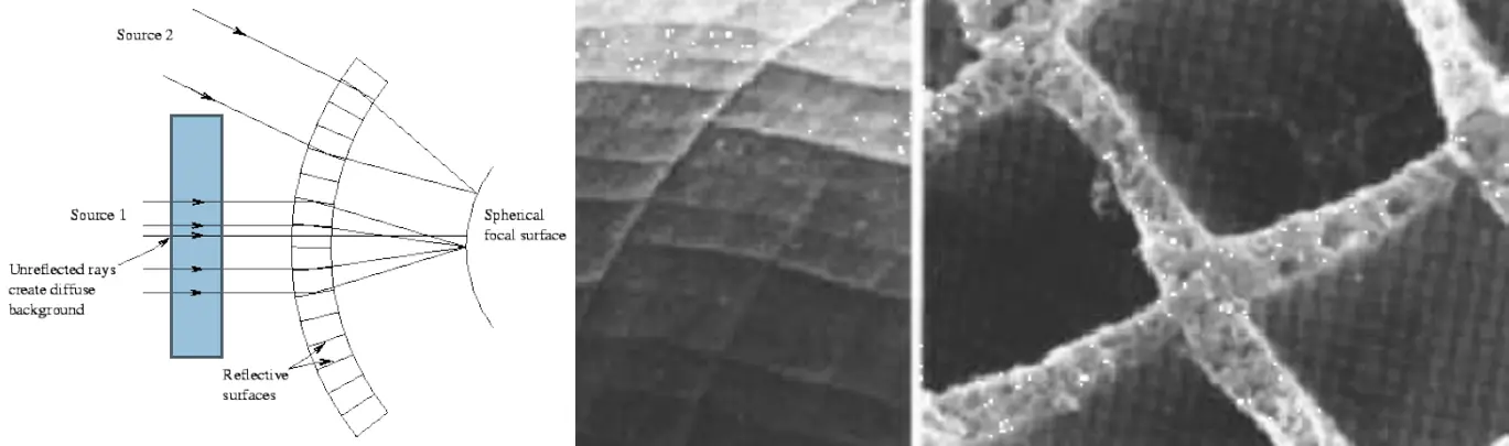
Arradiance has developed Noble metal ALD coatings, capable of achieving the required roughness for planar mirrors, optical components and within the high aspect ratio and high surface area of the Lobster eye device.
Joint Development Programs
Superconducting materials
Nano laminates
ALD Nanofilm technology can be used to deposit thin superconducting films that take advantage of its strengths and unique capabilities to create or enhance performance for a variety of applications, including high energy particle accelerators, superconducting wires for energy storage, and bolometers for radiation detection. Standard deposition methods for superconductors include physical vapor deposition (PVD), chemical vapor deposition (CVD), and molecular beam epitaxy (MBE) all have fundamental limitations, related to their physics that require line of sight deposition or result in non-uniform / non-conformal coverage. ALD, by its nature, deposits uniform conformal coatings over high aspect ratio structures and allows for unprecedented control of composition and thickness at the atomic level.
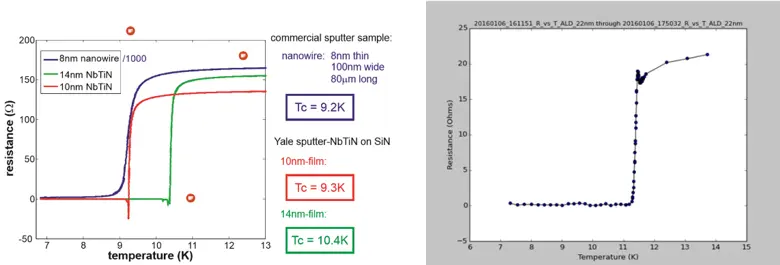
Arradiance has developed ALD transition metal-based superconductors, examples of which are nitrides of niobium, titanium, and Nano laminates (or hetero-structures) of the two. Plasma enhanced atomic layer deposition (PEALD) is used in this case for producing, pure, highly conducting transition metal nanofilms. The quality of a superconducting film is determined by the superconducting transition temperature (Tc). 14nm PVD-based NbTiN Nano laminates have demonstrated a Tc of 10.4K, figure right (green curve) while similar PVD results for a 10nm film producing a Tc of 9.3K. Researchers using PEALD have reported films with Tc values ranging from a few Kelvin up to 12.4K for 30nm thick films. Arradiance foundry has developed superconducting PEALD NbTiN hetero-structures deposited with (t-butylimido) tris(diethylamido) niobium(V) (TBTDEN), tetrakis(dimethylamino)titanium(IV) (TDMAT) and remote NH3 plasmas. A resistance vs. temperature plot of a 20nm NbTiN film deposited at 300C is shown in the gray graphic curve above. This film, which exhibited a room temperature resistivity of 325 mW-cm, had a Tc of 11.5K. Arradiance ALD superconducting nanofilms have achieved performance comparable to sputtered films. This results from films of exceptional purity, where oxygen (typically the major cause of Tc degradation) and carbon contamination is measured near or below the XPS detection threshold of (~1%).