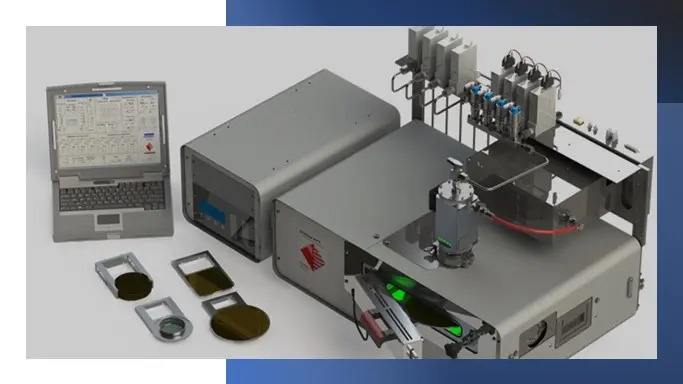
Arradiance is an Atomic Layer Deposition Company and a Supplier of Equipment and Foundry Services
Arradiance Header Logo

History of Arradiance

2004

History Icon

Founding

Originally founded as Emission Systems in 2003, Arradiance receives VC funding and a DARPA contract to develop a patented electron field emission array using a micro-channel technology

2005

History Icon

Silicon MCP Array

Arradiance demonstrates world’s first Micro-Channel Electron Amplification Array using Silicon Wafers

2007

History Icon

ALD Nano-engineered MCP

Arradiance demonstrates Nano-engineered ultra-high gain Microchannel plates using internally developed Atomic Layer Deposition equipment

2008

History Icon

GEM‐D2 ALD System

The GEM‐D2 to deposit atomically thin layers of material on virtually any substrate

2009

History Icon

Space Sciences Laboratory

University of California, Berkeley confirms a functional, uniform, and stable MCP using Arradiance ALD Technology

First plastic MCP

A Microchannel plate fabricated on a plastic substrate is demonstrated

2010

History Icon

GEMStar-6 ALD System

Arradiance Introduces Powerful New GEMStar Benchtop ALD System

NASA SBIR Grant

Received grant to develop new imaging and sensor technology using Arradiance’s proprietary GEM thin film technologies

2012

History Icon

GEMStar-8 ALD System

Arradiance Introduces New GEMStar Benchtop ALD System

Issued Multiple Patents

For Nanofilm technologies fundamental for large area MCP detection

2013

History Icon

MCP Technology Licensed

To ITT and INCOM For Arradiance patented ALD Microchannel plate (MCP) activation process for large-area MCP-photomultiplier tube (PMT) device

First Cryogenic MCP

Capable of MHz Signal Rate

2014

History Icon

GEMStar XT ALD Systems

Arradiance Introduces the First Benchtop Thermal and Plasma-Enhanced Atomic Layer Deposition System (PEALD) for material and device Research

2015

History Icon

MCP Technology Licensed

To Hamamatsu and PHOTEK LTD for Arradiance intellectual property for Atomic Layer Deposition (ALD) nanofilms for next generation MCP and photomultiplier tubes (PMT)

2016

History Icon

Michael D. Trotter

Joins Arradiance as Chief Executive Officer

2019

History Icon

Issued Multiple Patents

International patents for Nanofilm technology for noiseless low-signal amplification, critical to emerging scientific and commercial applications

New Facilities

10,000 sqft, a large clean room and 4,000 sqft manufacturing space

2020

History Icon

GEMStar Quantum

Arradiance Introduces GEMStar Quantum Atomic Layer Deposition Equipment Technology

Arradiance Icon

About Arradiance

Arradiance ALD Process Systems

Thank you for your interest in Arradiance

Specializing in Atomic Layer Deposition

Founded in 2003, we’ve been at the leading edge of Atomic Layer Deposition (ALD) and Plasma Enhanced Deposition (PEALD) technology for two decades

Contact Arradiance for additional information

Arradiance ALD Papers and Publications

Molecular Innovation™

Creating emerging technology worldwide

Our cutting-edge technology is trusted by the world’s leading research teams

  • View publications
  • Clean Energy
  • Energy Storage
  • Sensors
  • Micro Electronics
  • Nano Technology
  • Optoelectronics
  • Catalyst Systems

Management Team

Michael D. Trotter

Chief Executive Officer

Karen Buechler, PhD

Vice President, Business Development

Gargi Vaidya

General Manager, Operations

Huazhi Li, Ph.D

Manager, Foundry / Principal Scientist

Chan Im

Manager, Production and Procurement

Board of Directors

Thomas M. Clay

Chairman of the Board

Managing Member of Epacria Capital Partners

Michael D. Trotter

Board of Directors

CEO of Arradiance LLC

David R. Beaulieu

Board of Directors

Arradiance Founder

Managing Member of Fletcher Hill Innovations

Jeff Plante

Board of Directors

Chris Taylor

Board of Directors

President of Servantex LLC

Edward O’Neal

Inside Council and Secretary

Our customer's have said

Professor Chen Yang

Purdue University

“Purdue University was one of the earliest adopters of the Arradiance GEMStar XT-P Plasma PEALD system Our overall experience with the GEMStar XT-P Plasma system, service and support from Arradiance has been excellent

We would highly recommend that you contact Arradiance for your ALD or PEALD system and coating needs”

Dr. Chen Yang >

Professor Julien Bachmann

Friedrich-Alexander-Universität

“The Arradiance GEMStar-6 reactor has been in use in my laboratory for eight months continuously now and has performed consistently. It has worked from day one, and we have had no downtime at all so far, not even pump oil changes (with the exhaust abatement system). The chamber temperature is well controlled and the films are homogeneous.”

Dr. Julien Bachmann >

Professor Satoshi Uchida

University of Tokyo

“The Arradiance GEMStar-XT reactor in my laboratory is consistently producing high quality hole-blocking layer TiO2 film in my perovskite solar cell research. The ALD-based TiO2 layer through GEMStar-XT enables a high power conversion efficiency of 20% repeatedly and I am very pleased with the performance of GEMStar ALD tool”

Dr. Satoshi Uchida >

Director Casey Smith

Texas State University

“The Texas State University Nanofabrication Research Service Center is extremely pleased with the versatility of our GEMStar XT-DP PEALD System

The equipment is compact, economical, easily installed, well documented, and utilizes an intuitive user interface. Arradiance technical staff have rapidly responded to my requests for recipes and new chemistry support. To date we have trained more than 25 users in our shared cleanroom facility who have successfully deposited TiO2, Al2O3, ZnO, Al:ZnO, ZrO2, and/or SnO2”

Dr. Casey Smith >

Professor Andy Sun

Western University

“The GEMStar-8 ALD system is critical to our nanomaterials for clean energy research. In particular, the particle holder has been working perfectly for ALD coatings on nanostructured materials for Li batteries and fuel cells …… even better than expected”

Dr. Andy Sun >

Professor Meni Wanunu

Northeastern University

“We study the properties of biomolecules using various nanoscale systems. This requires the fabrication of uniform ultrathin freestanding membranes, some of which are deposited using our GEMStar ALD system. This system is small, easy to use, low-maintenance, and has been a workhorse for us – it just runs!”

Dr. Meni Wanunu >

Professor John Conley

Oregon State University

“GEMStar-6 has everything our lab environment should need in an ALD tool. It is small, flexible and can handle up to six inch wafers. We also like the 1” height of the chamber that accommodates small, three dimensional objects and the port we can use for in-situ metrology. The design appears to be rugged and easy to service.”

Dr. John F. Conley >

Steve Shepard

Facility Manager Boston College

“Much of our research is based around arrays of vertical nanostructures. The GEMStar ALD system allows us to deposit very uniform metallic and oxide thin films over these structures”

Steve Shepard >