Our deposition methods, in plain English.
Heard of ALD but aren’t a specialist? Start here. Three processes (ALD, PE-ALD, and MLD) describe what a film is made of. Two methods (temporal and spatial ALD) describe how it gets laid down. Then explore the systems and the published research that put them to work.
ALD, PE-ALD, and MLD at a glance.
What gets deposited. All three build a film one self-limiting cycle at a time; they differ in what each cycle leaves behind. How those cycles are delivered (temporal or spatial ALD) is a separate question, further down the page.
| Method | What it is | Best for |
|---|---|---|
| Atomic Layer Deposition (ALD) | Two precursor gases are pulsed in turn; each reacts only with the surface left by the last, one self-limiting cycle at a time. Builds inorganic films such as oxides, nitrides, metals. | Atomic-scale thickness control and conformal coating of deep trenches, pores, and 3D shapes for semiconductors, batteries, catalysts, and optics. |
| Plasma-enhanced ALD (PE-ALD) | ALD with a plasma to activate the reaction, for lower process temperatures and denser films. Works for nitrides and metals that thermal ALD struggles with. | Broader chemistry at lower temperature. Supported on the GEMStar XT-P and PRIME variants. |
| Molecular Layer Deposition (MLD) | ALD’s organic cousin. MLD builds organic and hybrid organic–inorganic layers from bifunctional organic molecules, one self-limiting step at a time. | Flexible, functional coatings for battery-electrode protection and tunable membranes. MLD and ALD run together can produce new functionalized nanomaterials. |
How ALD actually works.
How ALD & MLD relate to other thin-film deposition methods
ALD is CVD, split in two
ALD is a specialized form of chemical vapor deposition (CVD). In ordinary CVD, two precursors enter the chamber at once and react in the gas phase, growing film wherever they meet. ALD splits that single reaction into two half-reactions and separates the precursors in time: each is pulsed in, reacts only with the surface, then is purged away before the next arrives. That makes ALD a surface-mediated, self-limiting process rather than a gas-phase one.
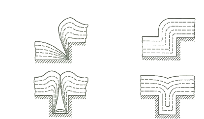 Diffusion-controlled (CVD)
Reaction-controlled (ALD)
Diffusion-controlled (CVD)
Reaction-controlled (ALD)
One growth cycle, step by step
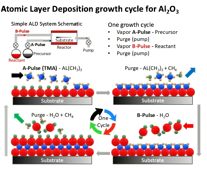
A single cycle adds a fraction of an atomic layer; the steps repeat until the target thickness is reached. Thermal Al₂O₃ growth is the classic example:
- Precursor pulse (A) — trimethylaluminum, Al(CH₃)₃, is pulsed in and bonds to the surface until every available site is filled, then stops. This self-limiting step is what gives ALD its atomic-scale control.
- Purge — inert gas and the pump clear excess precursor and the CH₄ by-product.
- Reactant pulse (B) — water vapor, H₂O, reacts with that layer to form Al₂O₃ and regenerate a fresh, reactive surface.
- Purge — excess water and by-products are pumped away, leaving the surface ready for the next cycle.
Why it matters: conformality
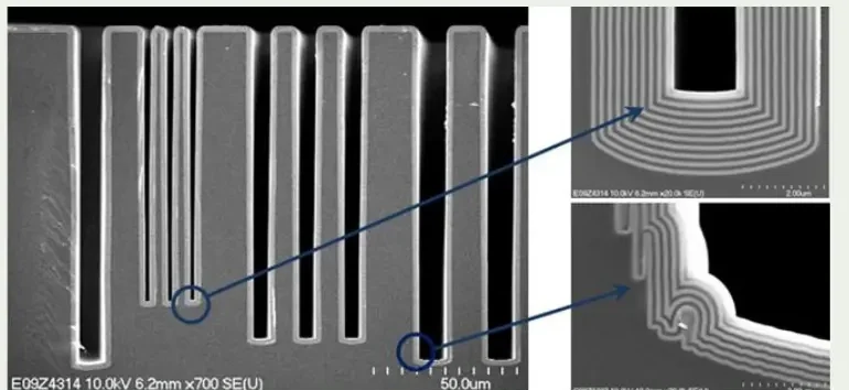
Because growth is limited by surface reactions rather than by how reactant diffuses in, as it is in CVD, every exposed surface is coated equally, even deep inside pores and high-aspect-ratio (large length-to-diameter) trenches. The payoff is conformal, pin-hole-free films of precisely controlled thickness on complex 3D geometry, such as alternating Ta₂O₅ and Al₂O₃ layers lining deep trenches in silicon. The same property is why ALD suits the fragile layer interfaces of perovskite solar cells, which our piece on perovskite interfaces explores.
Temporal and spatial ALD.
Everything above describes ALD separated in time. The same reactions can instead be separated in space. That change makes possible much faster deposition rates, which can help carry ALD from the research bench to the production line.
Temporal ALD: separated in time
The substrate sits still in one chamber, and the gases take turns. Precursor A is pulsed in, the chamber is purged, precursor B is pulsed in, and the chamber is purged again. The two half-reactions never meet in the gas phase because they never arrive at the same moment.
Those purge steps are what make the process work and also what make it slow: most of a cycle is spent clearing the chamber rather than growing film. At roughly a tenth of a nanometer per cycle, a 20 nm film is around 200 cycles, and each cycle is measured in seconds.
In research and low-volume production settings that is a fair trade. What the time buys is atomic-scale control over awkward geometry, such as deep trenches, porous media, powders, and one-off samples that change from week to week. This is how the GEMStar and PRIME systems work.
Spatial ALD: separated in space
Spatial ALD keeps the same two half-reactions apart by position instead. Both precursors flow continuously into different zones of the tool, held apart by curtains of inert gas rather than by purge steps. The substrate then moves — through zone A, across the curtain, through zone B, across the curtain — completing a full cycle on each pass.
The surface chemistry is unchanged. The reactions are the same self-limiting ones, and they still stop once every available site is filled. What disappears is the dead time: with no pump-and-purge between half-reactions, a cycle that took seconds can take hundredths of one, with the individual precursor and plasma exposures measured in thousandths of a second.
Spatial ALD itself can vary according to the substrate’s motion. Rotary ALD can sweep a wafer through zones arranged in a circle, while roll-to-roll ALD can move a web back and forth through zones arranged in a line. In a rotary arrangement, more than one precursor and plasma zone pair can be spaced around the same turntable, so a single revolution completes several full cycles rather than one.
| Characteristic | Temporal ALD | Spatial ALD |
|---|---|---|
| Precursors kept apart by | Time — a purge step between pulses. | Distance — inert gas curtains between zones. |
| What moves | The gases. The substrate stays put. | The substrate, passing each zone in turn. |
| One cycle is | A pulse–purge–pulse–purge sequence, typically seconds. | One pass through the zones, with the purge dead time removed. |
| Suits | Powders, one-off samples, and recipes that change from run to run, where flexibility matters more than throughput. | Repeat production of the same film: thick coatings, larger areas, and, for roll-to-roll ALD, flexible webs and sheets. |
Is it still ALD?
The obvious worry about running that fast is that it stops being ALD. The test is growth per cycle: if the reaction is genuinely self-limiting, each pass lays down the same amount of film however quickly the substrate travels. Push beyond the point where the zones stay properly separated, though, and the two precursors begin to meet in the gas phase. Growth per cycle then climbs, uniformity degrades, and the process has quietly become CVD. Saturated growth held steady across a range of speeds is the evidence that it has not.
What the fixed geometry changes
Because the substrate moves past a stationary electrode rather than sitting inside a chamber, a simple DC plasma source can be used, and it stays uniform however long that electrode is. The same arrangement therefore scales from a single wafer to a wide web without a different kind of plasma.
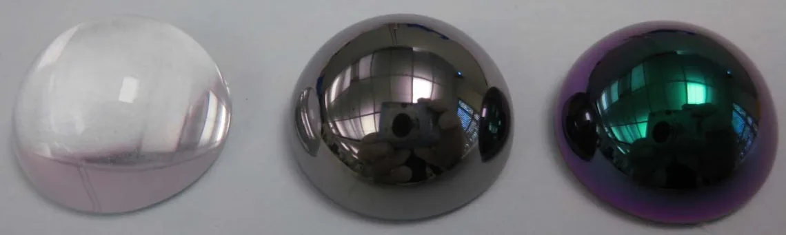
Holding the zones apart has traditionally meant keeping the coating head within a fraction of a millimeter of the substrate, which is why spatial ALD was long confined to flat, thin substrates. Relaxing that gap is what opens the method to taller three-dimensional parts, and published work now covers high-aspect-ratio trenches and millimeter-scale spheres at spatial speeds.
The two are complements rather than rivals. A process is usually proven on a temporal tool, where changing the recipe is cheap, then moved to a spatial one when the focus turns to depositing commercially relevant thicknesses over larger surface areas at acceptable time and cost.
Spatial ALD is the technology behind Arradiance’s combination with Lotus Applied Technology. Lotus AT has developed unique, patented intellectual property in rapid spatial and roll-to-roll ALD, enabling use cases impractical at the deposition speeds of traditional temporal ALD. Read what the combination means for customers of both companies, or Lotus AT’s own account of its technology at lotusat.com.
Recipes and films we routinely run.
A reference of common materials and the systems they run on. The full, searchable evidence base lives in the Research Library.
| Material | Type | Representative use |
|---|---|---|
| Al₂O₃ | Thermal / PE-ALD | Encapsulation, tunnel barriers, area-selective ALD |
| TiO₂ | Thermal / PE-ALD | Photocatalysis, optical layers, DNA sensing |
| SnO₂ | Thermal ALD | Perovskite solar-cell electron transport layers |
| ZnO | Thermal ALD | Antibacterial coatings, transparent conductors |
| Pt | Thermal / PE-ALD | Catalysis, electrodes |
| Lithicone (MLD) | MLD | Li-ion electrode protection |
Ready to talk specifics?
Tell us the film you need and the substrate it’s going on. We’ll point you to a system, a service, or the relevant published work.
Talk to a specialist